Metal-Organic Chemical Vapour Deposition (MOCVD)
Metal-Organic Chemical Vapour Deposition (MOCVD)
MOCVD is a chemical vapour deposition technique that uses metal-organic precursors to enable the growth of III-V semiconductors in two and three dimensions.
List of available equipment
TOOL MAKE AND MODEL
KEY DIFFERENTIATOR
LOCATION
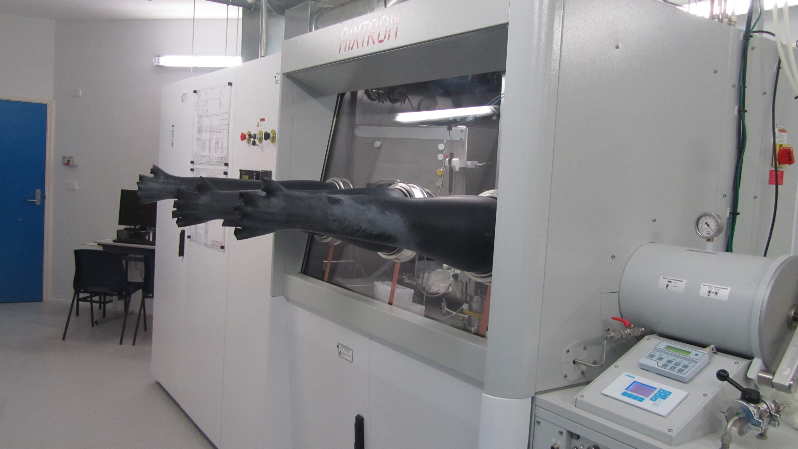
Aixtron 200/4
MOCVD (horizontal flow) system for epitaxial growth of III-V semiconductor structures.
ACT Node
Australian National University (ANU)
Description
Epitaxial growth of III-V (arsenide, phosphide and antimonide based materials) 2D and 3D semiconductor structures.
Related Information
A range of available sources (Ga, Al, In, Sn, Si, Zn, Sb and As, P) allows for the growth of wide range of semiconductor structures for various applications including metal catalysed nanostructures. Growth can be done on various substrates (GaAs, InP, InAs, GaP, Si etc.) and various crystal orientation up to 4" diameter and surface temperature up to 700C.
Tool Contact
horst.punzmann@anu.edu.au
Aixtron 3x2FT – Epitaxial growth of III-N
MOCVD CCS (Close-Coupled Showerhead) system for growth of III-nitride semiconductor structures
ACT Node
Australian National University (ANU)
Description
Epitaxial growth of III-N (nitride based materials) 2D and 3D semiconductor structures.
Related Information
A range of available sources (Ga, Al, In, B, Si, Mg, N) allows for the growth of wide range of semiconductor structures for various applications. Growth can be done on various substrates (Sapphire, Si, etc.) and various crystal orientation up to 4" diameter and surface temperature up to 1300C.
Tool Contact
horst.punzmann@anu.edu.au
Aixtron 3x2FT – Epitaxial growth of III-V
MOCVD CCS (Close-Coupled Showerhead) system for growth of III-V (III-As, III-P, III-Sb) semiconductor structures
ACT Node
Australian National University (ANU)
Description
Epitaxial growth of III-V (arsenide, phosphide and antimonide based materials) 2D and 3D semiconductor structures.
Related Information
A range of available sources (Ga, Al, In, C, Si, Mg, Zn, Sb and As, P in hydride and alkyl forms) allows for the growth of wide range of semiconductor structures for various applications. Growth can be done on various substrates (GaAs, InP, InAs, GaP, Si etc.) and various crystal orientation up to 4" diameter and surface temperature up to 800C.
Tool Contact
horst.punzmann@anu.edu.au
TOOL MAKE AND MODEL
KEY DIFFERENTIATOR
LOCATION
Aixtron 200/4
MOCVD (horizontal flow) system for epitaxial growth of III-V semiconductor structures.
ACT Node
Australian National University (ANU)
Description
Epitaxial growth of III-V (arsenide, phosphide and antimonide based materials) 2D and 3D semiconductor structures.
Related Information
A range of available sources (Ga, Al, In, Sn, Si, Zn, Sb and As, P) allows for the growth of wide range of semiconductor structures for various applications including metal catalysed nanostructures. Growth can be done on various substrates (GaAs, InP, InAs, GaP, Si etc.) and various crystal orientation up to 4" diameter and surface temperature up to 700C.
Tool Contact
horst.punzmann@anu.edu.au
TOOL MAKE AND MODEL
KEY DIFFERENTIATOR
LOCATION
Aixtron 3x2FT – Epitaxial growth of III-N
MOCVD CCS (Close-Coupled Showerhead) system for growth of III-nitride semiconductor structures
ACT Node
Australian National University (ANU)
Description
Epitaxial growth of III-N (nitride based materials) 2D and 3D semiconductor structures.
Related Information
A range of available sources (Ga, Al, In, B, Si, Mg, N) allows for the growth of wide range of semiconductor structures for various applications. Growth can be done on various substrates (Sapphire, Si, etc.) and various crystal orientation up to 4" diameter and surface temperature up to 1300C.
Tool Contact
horst.punzmann@anu.edu.au
TOOL MAKE AND MODEL
KEY DIFFERENTIATOR
LOCATION
Aixtron 3x2FT – Epitaxial growth of III-V
MOCVD CCS (Close-Coupled Showerhead) system for growth of III-V (III-As, III-P, III-Sb) semiconductor structures
ACT Node
Australian National University (ANU)
Description
Epitaxial growth of III-V (arsenide, phosphide and antimonide based materials) 2D and 3D semiconductor structures.
Related Information
A range of available sources (Ga, Al, In, C, Si, Mg, Zn, Sb and As, P in hydride and alkyl forms) allows for the growth of wide range of semiconductor structures for various applications. Growth can be done on various substrates (GaAs, InP, InAs, GaP, Si etc.) and various crystal orientation up to 4" diameter and surface temperature up to 800C.
Tool Contact
horst.punzmann@anu.edu.au