
Quantum computing
Quantum computers are expected to bring around a technological revolution once built to scale, outperforming conventional computers in many important areas and assisting drug development, simulations, weather modelling, and cybersecurity applications.
Researchers across the world are working to build the fundamental components of a quantum computer, a qubit (quantum bit), that can be used in the real world.
Silicon is proving to be a promising foundation for building functional qubits. In a silicon quantum bit (qubit), single trapped electrons are used to represent binary code and allow the quantum computer to perform calculations. Such devices, which closely resemble modern day CMOS transistors, use nanoscale gate electrodes to confine and control electron spins to form universal quantum logic gates, which are fundamental building blocks for a quantum processor.
List of Possible Process Flows
Silicon MOS device fabrication
Step 1
Step 2
Step 3
Step 4
Step 5
Spin coating and wafer development
Spin coaters are capable of applying uniform thickness polymer films, such as a resist to substrates. Resist is essential for many types of lithography, such as UV lithography. Resists are termed either positive or negative — this denotes whether, when cured, chemical bonds are made or broken, and therefore whether…
Electron Beam Lithography (EBL)
Electron Beam Lithography (EBL) allows users to write patterns with extremely high resolution, smaller than 10nm in size. It makes use of a highly energetic, tightly focused electron beam, which is scanned over a sample coated with an electron-sensitive resist. The electron beam scans the image according to a…
Electron Beam Evaporation (E-Beam Evaporation)
Electron-beam evaporation is a physical vapour deposition method for depositing thin films of metals, oxides and semiconductors in a high vacuum environment. Ultra high purity coating material is placed inside a vacuum chamber, typically as pellets in a crucible. Electron energy is used to heat these pellets,…
Wetbench
A wetbench is a potentially automated process tool that is used to carry out wet etching or cleaning steps of a fabrication process.
Scanning Electron Microscopy (SEM)
Scanning Electron Microscopy (SEM) is the process whereby a tightly focused electron beam is scanned onto the surface to be imaged. As the primary electrons hit the atoms in the surface, a number of secondary electrons are emitted, and collected by the instrument’s detector, which assigns a level of grey…
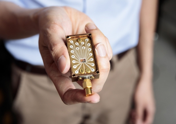
Device packaging and bonding
Step 1
Step 2
Step 3
Wafer dicing
Nanofabricated devices are generally made in batches on wafers and need to be separated or packaged before use. This separation can be achieved through wet or dry dicing. In a wet dicing operation, a precision, high-speed, diamond impregnated blade is used to mill narrow grooves between the devices either partially…
Wetbench
A wetbench is a potentially automated process tool that is used to carry out wet etching or cleaning steps of a fabrication process.
Wire bonding
Wire bonding is the part of the fabrication that allows an electrical component to communicate with the outside world. A thin electrically conductive wire – typically gold, aluminium, copper or silver – is used to allow electricity to flow from contacts on the component to, or from, its packaging.
There are…