
Micro-electro-mechanical systems (MEMS)
MEMS, or micro-electro-mechanical systems, is a broad class of technologies that make use of micromachined structures, sensors, and moving parts. They often perform tasks that range from detecting changes in temperature or pressure, to tuning light sensors or manoeuvring mirrors.
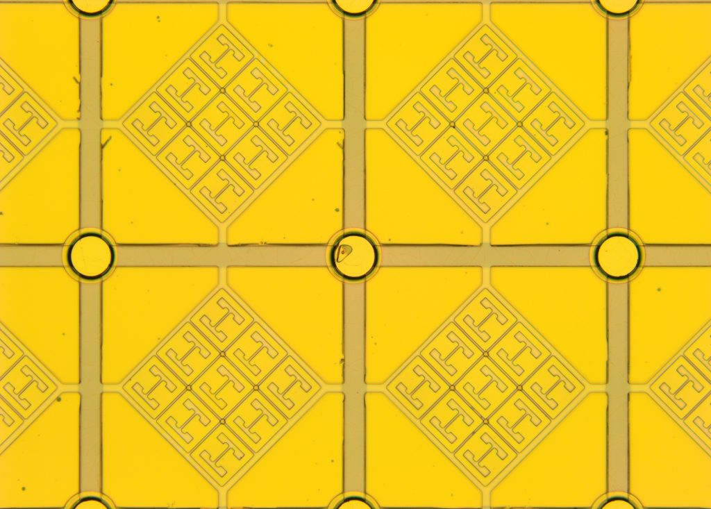
MEMS often feature incredibly intricate designs with part dimensions between 100 nm to 100 µm. The fabrication process involves multiple steps of deposition, lithography, and etching to create layers upon layers of patterned material that result in a desired structure.
MEMS-based devices are widely applied but their robustness, sensitivity, and small footprint make them particularly useful for sensing applications in the field – for instance in the agricultural industry where they are being used in combination with drone technology to monitor crop wellbeing by providing multispectral information over large areas. Other uses include to both detect and produce sound in consumer electronics, as accelerometers in the automotive industry, or to control light signals in the communication.
List of Possible Process Flows
Fabricating ~100nm structures
Step 1
Step 2
Step 3
Step 4
Electron Beam Lithography (EBL)
Electron Beam Lithography (EBL) allows users to write patterns with extremely high resolution, smaller than 10nm in size. It makes use of a highly energetic, tightly focused electron beam, which is scanned over a sample coated with an electron-sensitive resist. The electron beam scans the image according to a…
Electron Beam Evaporation (E-Beam Evaporation)
Electron-beam evaporation is a physical vapour deposition method for depositing thin films of metals, oxides and semiconductors in a high vacuum environment. Ultra high purity coating material is placed inside a vacuum chamber, typically as pellets in a crucible. Electron energy is used to heat these pellets,…
Reactive Ion Etching (RIE)
Reactive Ion Etching (RIE) is a method that combines both chemical and physical etching to allow isotropic and anisotropic material removal.
The etching process is carried out in a chemically reactive plasma containing positively and negatively charged ions generated from gases that are pumped into the reaction…
Scanning Electron Microscopy (SEM)
Scanning Electron Microscopy (SEM) is the process whereby a tightly focused electron beam is scanned onto the surface to be imaged. As the primary electrons hit the atoms in the surface, a number of secondary electrons are emitted, and collected by the instrument’s detector, which assigns a level of grey…
Fabricating ~100µm structures
Step 1
Step 2
Step 3
Step 4
Step 5
Spin coating and wafer development
Spin coaters are capable of applying uniform thickness polymer films, such as a resist to substrates. Resist is essential for many types of lithography, such as UV lithography. Resists are termed either positive or negative — this denotes whether, when cured, chemical bonds are made or broken, and therefore whether…
Multiple mask lithography
Photolithography is used to create a pattern on a substrate by shining light from a light source onto a photoresist that coats the surface of the substrate through a photomask and is followed by a development phase.
Depending on the complexity of a device’s design, various deposition, etching and lithography…
Atomic Layer Deposition (ALD)
Atomic Layer Deposition (ALD) involves the deposition of materials one atomic monolayer at a time. It forms extremely uniform, conformal, pin-hole-free coatings even on high-aspect-ratio structures. This is achieved by pulsing a chemical precursor onto a hydroxylated substrate surface which reacts, resulting in a…
Reactive Ion Etching (RIE)
Reactive Ion Etching (RIE) is a method that combines both chemical and physical etching to allow isotropic and anisotropic material removal.
The etching process is carried out in a chemically reactive plasma containing positively and negatively charged ions generated from gases that are pumped into the reaction…
Atomic Force Microscopy (AFM)
Atomic force microscopy (AFM) is one of the most versatile characterisation methods.
AFM performs scanning probe microscopy, scanning the surface of a material with a nanoscale cantilever, either through direct contact or through oscillating the cantilever just above the surface. When the cantilever is positioned…