ANFF Victoria
Home > Locations
Overview

ANFF-Vic ties the largest open-access cleanroom in the southern hemisphere, the Melbourne Centre for Nanofabrication (MCN), with five university-based hubs and CSIRO spread across Victoria providing a full complement of nanofabrication capabilities and expertise.

Members of the ANFF-Vic Joint Venture include: Monash University; University of Melbourne (Materials Characterisation and Fabrication Platform); Deakin University (Institute for Frontier Materials); La Trobe University (Centre for Materials Surface Science); Swinburne University of Technology (ANFF Biointerface Engineering Hub); RMIT University (Micro Nano Research Facility); Victoria University; and CSIRO (CSIRO Manufacturing).

MCN

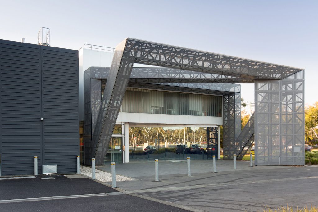
The Melbourne Centre for Nanofabrication is home to ANFF’s headquarters. The Centre is a world-class, purpose-built facility boasting state-of-the-art cleanrooms (class 10,000 and class 100), reconfigurable biochemistry and PC2 labs, a microscopy lab and focused ion beam lab. These specialised work environments house top-of-the-line micro and nanofabrication equipment and instrumentation.

Node Competencies

Current expertise is provided in the areas of advanced materials and biotechnology, leading to the development of a wide range of customised sensors, actuators, and devices applied to areas from biomedicine, and energy to nanoelectronics and the environment.

Contact

Node Director: Prof Nico Voelcker
Email: nicolas.voelcker@monash.edu
Phone: +61 3 9902 9097

General Manager: Dr Sean Langelier
Email: sean.langelier@nanomelbourne.com
Phone: +61 3 9902 4100

Location
Melbourne Centre for Nanofabrication
Address

Melbourne Centre for Nanofabrication
151 Wellington Road
Clayton VIC 3168

Website

Deakin University
Address

Institute for Frontier Materials
Deakin University, Waurn Ponds Campus
Waurn Ponds VIC 3216

Website

University of Melbourne
Address

Materials Characterisation and Fabrication Platform
The University of Melbourne
Parkville Victoria 3010

Website

La Trobe University
Address

Centre for Materials and Surface Science (CMSS)
Department of Chemistry and Physics
La Trobe University
Bundoora VIC 3086

Website

Swinburne University of Technology
Address

ANFF-Vic Biointerface Engineering Hub
Swinburne University of Technology
John Street
Hawthorn Victoria 3122

Website

RMIT
Address

MicroNano Research Facility
RMIT University
Bowen Street
Melbourne 3001 Victoria

Website

CSIRO
Address

CSIRO Clayton

Research Way, Clayton VIC 3168

Website

Equipment
Deposition
Anatech Hummer BC-20
RF/DC sputtering system
Melbourne Centre for Nanofabrication VIC Node
Technique
Sputtering
Description
Manual tool which can be used to deposit a wide variety of conductive and non-conductive thin films including metals, oxides, nitrides and alloys. The system allows for up to two materials to be co-deposited at once, with the option to vary the composition over time.
Related Information
Can coat with two materials in the same run.Features ion beam cleaning.Manual operation.Can be used to coat samples of up to 6 inches in diameter.
Tool Contact
mcn-enquiries@nanomelbourne.com
Intlvac Nanochrome
AC/DC Sputtering system with co-deposition
Melbourne Centre for Nanofabrication VIC Node
Technique
Sputtering
Description
An automated tool which can be used to deposit a wide variety of conductive thin films including metals, oxides, nitrides and alloys. The system allows for up to three materials to be co-deposited at once, with the option to vary the composition over time.
Related Information
Can coat with three materials in the same run.Features ion beam cleaning.Recipe-based automated operation.Can be used to coat samples of up to 8 inches in diameter.
Tool Contact
mcn-enquiries@nanomelbourne.com
Oxford Instruments Plasmalab 100 ICP380 – PECVD setup
Plasma enhanced chemical vapour deposition system (PECVD) for depositing SiOx and SiN
Melbourne Centre for Nanofabrication VIC Node
Technique
Plasma Enhanced Chemical Vapour Deposition (PECVD)
Description
Offers fast, affordable deposition at relatively low temperatures.
Related Information
Deposits SiO2, Si3N4, and amorphous Silicon at 100-400 degrees C.
Tool Contact
mcn-enquiries@nanomelbourne.com
Seki AX6300
MPCVD system for deposition of boron-doped diamond
Melbourne Centre for Nanofabrication VIC Node
Technique
Microwave Plasma-enhanced Chemical Vapour Deposition (MPCVD)
Description
Used to coat seeded samples of any shape with boron-doped diamond.
Related Information
Deposits at approximately 1 µm/h.Maximum sample size is 2 inches.
Tool Contact
mcn-enquiries@nanomelbourne.com
Digital Matrix SA1000
Nickel electroplating system
Melbourne Centre for Nanofabrication VIC Node
Technique
Electroplating
Description
Can fabricate Ni master mould from patterned (photolithography, EBL) substrates to be used in hot embossing and nano-imprint lithography for mass production
Related Information
Up to 8 inch diameter sample size; mould thickness up to 1 micron, minimum feature size depends on aspect ratio
Tool Contact
mcn-enquiries@nanomelbourne.com
Intlvac Nanochrome II
Electron beam evaporator
Melbourne Centre for Nanofabrication VIC Node
Technique
Electron Beam Evaporation (E-Beam Evaporation)
Description
Single films or multi-material stacks are easily created using simple layer definitions. Features ion-beam pre-cleaning and sample heating capabilities.
Related Information
Features a 10kV power supply and supports up to sixteen 4 inch wafers or fifteen 6 inch wafers or wafer mounted samples.Coating thickness are from 2nm up to 200nm (thickness >200nm by approval). Currently available in the materials library are metals (Al, Cr, Ti, Au, Ag), oxides (SiO2, TiO2, Al2O3, ITO), fluorides (MgF2) and semiconductors (Si, Ge).
Tool Contact
mcn-enquiries@nanomelbourne.com
Cambridge NanoTech Fiji 200
Plasma assisted atomic layer deposition (PA-ALD) System
Melbourne Centre for Nanofabrication VIC Node
Technique
Atomic Layer Deposition (ALD)
Description
The Fiji F200 is capable of both thermal and Plasma Assisted ALD (PA-ALD). PA-ALD expands the window for materials by decreasing activation energy and allows for deposition at lower temperatures to reduce precursor decomposition, deposition times and film contaminations. This tool is equipped to enable Cambridge Nanotech’s unique Exposure Mode™ for thin film deposition on ultra high aspect ratio substrates. In-situ film growth can be monitored using a spectroscopic ellipsometry.
Related Information
Substrate size - Up to 6 inch diameter. Maximum substrate heating - 500°C. Available ALD films- Al2O3, TiO2, SiO2, SnO2, ZnO, Ta2O5, MoO3, HfO2, TiN, AZO.
Tool Contact
mcn-enquiries@nanomelbourne.com
Cambridge NanoTech Savannah S100
Atomic layer deposition (ALD) system in a glovebox
Melbourne Centre for Nanofabrication VIC Node
Technique
Atomic Layer Deposition (ALD)
Description
This glovebox-integrated thermal ALD system allows the user to deposit materials in controlled environments.
Related Information
Available films- Al2O3, TiO2, WO3, NiOx. Compatible up to 4 inch diameter sample size
Tool Contact
mcn-enquiries@nanomelbourne.com
TOOL MAKE AND MODEL
KEY DIFFERENTIATOR
LOCATION
TOOL MAKE AND MODEL
KEY DIFFERENTIATOR
LOCATION
Anatech Hummer BC-20
RF/DC sputtering system
Melbourne Centre for Nanofabrication VIC Node
Description
Manual tool which can be used to deposit a wide variety of conductive and non-conductive thin films including metals, oxides, nitrides and alloys. The system allows for up to two materials to be co-deposited at once, with the option to vary the composition over time.
Related Information
Can coat with two materials in the same run.Features ion beam cleaning.Manual operation.Can be used to coat samples of up to 6 inches in diameter.
Tool Contact
mcn-enquiries@nanomelbourne.com
TOOL MAKE AND MODEL
KEY DIFFERENTIATOR
LOCATION
Intlvac Nanochrome
AC/DC Sputtering system with co-deposition
Melbourne Centre for Nanofabrication VIC Node
Description
An automated tool which can be used to deposit a wide variety of conductive thin films including metals, oxides, nitrides and alloys. The system allows for up to three materials to be co-deposited at once, with the option to vary the composition over time.
Related Information
Can coat with three materials in the same run.Features ion beam cleaning.Recipe-based automated operation.Can be used to coat samples of up to 8 inches in diameter.
Tool Contact
mcn-enquiries@nanomelbourne.com
TOOL MAKE AND MODEL
KEY DIFFERENTIATOR
LOCATION
Oxford Instruments Plasmalab 100 ICP380 – PECVD setup
Plasma enhanced chemical vapour deposition system (PECVD) for depositing SiOx and SiN
Melbourne Centre for Nanofabrication VIC Node
Description
Offers fast, affordable deposition at relatively low temperatures.
Related Information
Deposits SiO2, Si3N4, and amorphous Silicon at 100-400 degrees C.
Tool Contact
mcn-enquiries@nanomelbourne.com
TOOL MAKE AND MODEL
KEY DIFFERENTIATOR
LOCATION
Seki AX6300
MPCVD system for deposition of boron-doped diamond
Melbourne Centre for Nanofabrication VIC Node
Description
Used to coat seeded samples of any shape with boron-doped diamond.
Related Information
Deposits at approximately 1 µm/h.Maximum sample size is 2 inches.
Tool Contact
mcn-enquiries@nanomelbourne.com
TOOL MAKE AND MODEL
KEY DIFFERENTIATOR
LOCATION
Digital Matrix SA1000
Nickel electroplating system
Melbourne Centre for Nanofabrication VIC Node
Description
Can fabricate Ni master mould from patterned (photolithography, EBL) substrates to be used in hot embossing and nano-imprint lithography for mass production
Related Information
Up to 8 inch diameter sample size; mould thickness up to 1 micron, minimum feature size depends on aspect ratio
Tool Contact
mcn-enquiries@nanomelbourne.com
TOOL MAKE AND MODEL
KEY DIFFERENTIATOR
LOCATION
Intlvac Nanochrome II
Electron beam evaporator
Melbourne Centre for Nanofabrication VIC Node
Description
Single films or multi-material stacks are easily created using simple layer definitions. Features ion-beam pre-cleaning and sample heating capabilities.
Related Information
Features a 10kV power supply and supports up to sixteen 4 inch wafers or fifteen 6 inch wafers or wafer mounted samples.Coating thickness are from 2nm up to 200nm (thickness >200nm by approval). Currently available in the materials library are metals (Al, Cr, Ti, Au, Ag), oxides (SiO2, TiO2, Al2O3, ITO), fluorides (MgF2) and semiconductors (Si, Ge).
Tool Contact
mcn-enquiries@nanomelbourne.com
TOOL MAKE AND MODEL
KEY DIFFERENTIATOR
LOCATION
Cambridge NanoTech Fiji 200
Plasma assisted atomic layer deposition (PA-ALD) System
Melbourne Centre for Nanofabrication VIC Node
Description
The Fiji F200 is capable of both thermal and Plasma Assisted ALD (PA-ALD). PA-ALD expands the window for materials by decreasing activation energy and allows for deposition at lower temperatures to reduce precursor decomposition, deposition times and film contaminations. This tool is equipped to enable Cambridge Nanotech’s unique Exposure Mode™ for thin film deposition on ultra high aspect ratio substrates. In-situ film growth can be monitored using a spectroscopic ellipsometry.
Related Information
Substrate size - Up to 6 inch diameter. Maximum substrate heating - 500°C. Available ALD films- Al2O3, TiO2, SiO2, SnO2, ZnO, Ta2O5, MoO3, HfO2, TiN, AZO.
Tool Contact
mcn-enquiries@nanomelbourne.com
TOOL MAKE AND MODEL
KEY DIFFERENTIATOR
LOCATION
Cambridge NanoTech Savannah S100
Atomic layer deposition (ALD) system in a glovebox
Melbourne Centre for Nanofabrication VIC Node
Description
This glovebox-integrated thermal ALD system allows the user to deposit materials in controlled environments.
Related Information
Available films- Al2O3, TiO2, WO3, NiOx. Compatible up to 4 inch diameter sample size
Tool Contact
mcn-enquiries@nanomelbourne.com
Etching
Oxford Instruments Plasmalab 100 ICP380 – Silicon-specific dry etching
Deep reactive ion etcher (DRIE) capable of Bosch process
Melbourne Centre for Nanofabrication VIC Node
Technique
Deep Reactive Ion Etching (DRIE)
Description
Silicon-specific dry etching with good control over feature size and Bosch process capability for high aspect ratio structures.
Related Information
SF6 gas is turned in to a plasma using RF power. The plasma that is created is highly reactive to Silicon. The SF6 combined with a passivating chemistry using C4F8, which is used to control the Silicon etching profile.
Tool Contact
mcn-enquiries@nanomelbourne.com
Oxford Instruments Plasmalab 100 ICP380 DRIE setp
Deep reactive ion etcher (DRIE)
Melbourne Centre for Nanofabrication VIC Node
Technique
Deep Reactive Ion Etching (DRIE)
Description
General dry reactive etching of wide range of materials.
Related Information
Reactive species and ions are used to react with the substrate that is placed in the reactor to etch Si, SiO2, SI3N4, SiC, a-Si, Ti, TiW, Mo, Nb, Ta, Graphene and other 2D materials, Cr, Au, LiNbO3, Al, Al2O3, Hf, Hf02, TiN, TiO2, and more.
Tool Contact
mcn-enquiries@nanomelbourne.com
TOOL MAKE AND MODEL
KEY DIFFERENTIATOR
LOCATION
TOOL MAKE AND MODEL
KEY DIFFERENTIATOR
LOCATION
Oxford Instruments Plasmalab 100 ICP380 – Silicon-specific dry etching
Deep reactive ion etcher (DRIE) capable of Bosch process
Melbourne Centre for Nanofabrication VIC Node
Description
Silicon-specific dry etching with good control over feature size and Bosch process capability for high aspect ratio structures.
Related Information
SF6 gas is turned in to a plasma using RF power. The plasma that is created is highly reactive to Silicon. The SF6 combined with a passivating chemistry using C4F8, which is used to control the Silicon etching profile.
Tool Contact
mcn-enquiries@nanomelbourne.com
TOOL MAKE AND MODEL
KEY DIFFERENTIATOR
LOCATION
Oxford Instruments Plasmalab 100 ICP380 DRIE setp
Deep reactive ion etcher (DRIE)
Melbourne Centre for Nanofabrication VIC Node
Description
General dry reactive etching of wide range of materials.
Related Information
Reactive species and ions are used to react with the substrate that is placed in the reactor to etch Si, SiO2, SI3N4, SiC, a-Si, Ti, TiW, Mo, Nb, Ta, Graphene and other 2D materials, Cr, Au, LiNbO3, Al, Al2O3, Hf, Hf02, TiN, TiO2, and more.
Tool Contact
mcn-enquiries@nanomelbourne.com
Laboratory Infrastructure
Amerimade Automated Wetbench Suite
Set of wet benches for wet processing
Melbourne Centre for Nanofabrication VIC Node
Technique
Wetbench
Description
The automated wet-bench suite is comprised of three custom made instruments – a manual wet processing deck, a semi-automated chemical cleaning station and an IPA aerosol vapour dryer. All three wetbench instruments are designed to accommodate 25 wafers processing at a time resulting in high throughput and large volume of chemical ensure repeatable results. The wetbench suite significantly reduces the risk of using dangerous chemical by eliminating beakers and safe waste management systems.
Related Information
Manual wet processing baths - KOH, Cr etcher, 5% H2SO4, IPA and DI water. Semi-automated chemical cleaning station (enclosed, exhausted) baths - piranha, SC-2, buffered oxide etch (BOE), DI water and ultrasonic acetone de-scum station. The IPA aerosol vapour dryer dries without any need for heaters or rotation. Substrate size - Up to 6 ". Batch processing - Up to 25 wafers.
Tool Contact
mcn-enquiries@nanomelbourne.com
MBraun MB200
Glovebox for solar cells with ALD and electron beam evaporator
Melbourne Centre for Nanofabrication VIC Node
Technique
Gloveboxes
Description
A glovebox facility with ALD and Savannah S100 electron beam evaporator.
Related Information
Useful for oxygen-sensitive chemistries and the assembly of organic photovoltaics and flexible transistor fabrication.
Tool Contact
mcn-enquiries@nanomelbourne.com
Fumehoods Biological Safety Cabinets
Topsafe Class II
Melbourne Centre for Nanofabrication VIC Node
Technique
Fumehoods
Description
A recirculating fume cupboard with a spin coater and a hot plate.
Related Information
Standard equipment for photolithography, using a wide range of photoresists (AZ, SU8, PPA, PMMA) and various substrates.
Tool Contact
mcn-enquiries@nanomelbourne.com
TOOL MAKE AND MODEL
KEY DIFFERENTIATOR
LOCATION
TOOL MAKE AND MODEL
KEY DIFFERENTIATOR
LOCATION
Amerimade Automated Wetbench Suite
Set of wet benches for wet processing
Melbourne Centre for Nanofabrication VIC Node
Description
The automated wet-bench suite is comprised of three custom made instruments – a manual wet processing deck, a semi-automated chemical cleaning station and an IPA aerosol vapour dryer. All three wetbench instruments are designed to accommodate 25 wafers processing at a time resulting in high throughput and large volume of chemical ensure repeatable results. The wetbench suite significantly reduces the risk of using dangerous chemical by eliminating beakers and safe waste management systems.
Related Information
Manual wet processing baths - KOH, Cr etcher, 5% H2SO4, IPA and DI water. Semi-automated chemical cleaning station (enclosed, exhausted) baths - piranha, SC-2, buffered oxide etch (BOE), DI water and ultrasonic acetone de-scum station. The IPA aerosol vapour dryer dries without any need for heaters or rotation. Substrate size - Up to 6 ". Batch processing - Up to 25 wafers.
Tool Contact
mcn-enquiries@nanomelbourne.com
TOOL MAKE AND MODEL
KEY DIFFERENTIATOR
LOCATION
MBraun MB200
Glovebox for solar cells with ALD and electron beam evaporator
Melbourne Centre for Nanofabrication VIC Node
Description
A glovebox facility with ALD and Savannah S100 electron beam evaporator.
Related Information
Useful for oxygen-sensitive chemistries and the assembly of organic photovoltaics and flexible transistor fabrication.
Tool Contact
mcn-enquiries@nanomelbourne.com
TOOL MAKE AND MODEL
KEY DIFFERENTIATOR
LOCATION
Fumehoods Biological Safety Cabinets
Topsafe Class II
Melbourne Centre for Nanofabrication VIC Node
Description
A recirculating fume cupboard with a spin coater and a hot plate.
Related Information
Standard equipment for photolithography, using a wide range of photoresists (AZ, SU8, PPA, PMMA) and various substrates.
Tool Contact
mcn-enquiries@nanomelbourne.com
Lithography
ABM Stand Alone UV Exposure System
UV flood exposure source
Melbourne Centre for Nanofabrication VIC Node
Technique
UV Flood Exposure
Description
A versatile system that floods the exposure chamber with UV light.
Related Information
This equipment can produce features that measure ~2 µm in size.A 7-inch sample well allows for versatility and processing of relatively large or abnormally shaped substrates and samples.Most substrate materials can be used.
Tool Contact
mcn-enquiries@nanomelbourne.com
SwissLitho NanoFrazor
Thermal Scanning Probe Lithography (t-SPL) system
Melbourne Centre for Nanofabrication VIC Node
Technique
Thermal Scanning Probe Lithography (t-SPL)
Description
Operates at ambient temperature, pressure, low voltage, and under N2 atmosphere.Not reliant on ion gun or electron beam which is good when processing sensitive materials and devices.
Related Information
Uses a 1,000°C cantilever tip to sublimate PPA resist.Sub -10nm resolution, <2nm vertical accuracy
Tool Contact
mcn-enquiries@nanomelbourne.com
PicoTRACK PCT-150RRE
Automated spin-coating and wafer developing system
Melbourne Centre for Nanofabrication VIC Node
Technique
Spin coating and wafer development
Description
A fully automated system for wafer processing which includes spin coating, HMDS application, baking, and development.The system is well suited to batch scale production, providing high process performance and consistency in coating and development.
Related Information
Substrate size - 4 and 6 inch wafers. Batch process size - up to 25 wafers at a time. Resist system used - AZ 1512 and AZ 4562 photoresists to coat wafers and AZ 400K for development.
Tool Contact
mcn-enquiries@nanomelbourne.com
Suss Delta RC80+ Spin Coater
Spin coater
Melbourne Centre for Nanofabrication VIC Node
Technique
Spin coating and wafer development
Description
Spin coater set up to process 4-inch wafers and also features a hot plate.
Related Information
high uniformity spin coater.
Tool Contact
mcn-enquiries@nanomelbourne.com
EVG 620
Mask aligner and resist exposure system with NIL capability
Melbourne Centre for Nanofabrication VIC Node
Technique
Nano Imprint Lithography
Description
A high-resolution mask aligner with split-field microscopes that is capable of handling multiple wafer sizes with quick change-over time. Features back side alignment capability for mask aligning.
Related Information
Used for a variety of applications to transfer multiple layers of nanoscale patterns into photoresist films.Provides a minimum feature size of approximately 1 µm.
Tool Contact
mcn-enquiries@nanomelbourne.com
Intelligent Micropatterning SF100 XPRESS
Maskless micropatterning system
Melbourne Centre for Nanofabrication VIC Node
Technique
Maskless lithography
Description
A maskless photolithography system capable of writing features down to 1 μm, that offers speed and cost benefits over masked systems.
Related Information
A wide range of materials can be processed, and provides great control in writing and aligning fine features on smaller substrates. The process us non-contact, which reduces risk of damaged samples. Commonly used to quickly and accurately create photomasks.
Tool Contact
mcn-enquiries@nanomelbourne.com
EVG 520
Hot embossing tool
Melbourne Centre for Nanofabrication VIC Node
Technique
Hot embossing
Description
Can emboss wafers and perform bonding such as anodic bonding, fusion bonding, eutectic bonding and epoxy bonding.
Related Information
Used for controlled embossing into polycarbonate and COC substrates of up to 6 inches in diameter.
Tool Contact
mcn-enquiries@nanomelbourne.com
FEI Helios NanoLab 600 Dual Beam
Scanning electron microscope with focused ion beam for milling (FIB-SEM)
Melbourne Centre for Nanofabrication VIC Node
Technique
Focused Ion Beam (FIB) milling
Description
Ultra-high resolution three dimensional imaging for topography, surface morphology and maskless ion beam direct lithography.
Related Information
Ultra-high resolution imaging of samples of all sizes up to 6-inch wafers. The 5-axis stage and 100mm stage movement add flexibility to this equipment. Choice of Secondary Electrons (SE) detector best for topography images and Back-Scattered Electrons (BSE) detector for studies of features deep beneath the surface. Ion beam patterning with 30 kV accelerating voltage and variable currents.
Tool Contact
mcn-enquiries@nanomelbourne.com
Vistec EBL 5000
Electron beam lithography (EBL) system
Melbourne Centre for Nanofabrication VIC Node
Technique
Electron Beam Lithography (EBL)
Description
EBL that is capable of exposing thick layers of e-beam resist of up to several micrometres with small forward scattering.Fully automated equipment features a laser height measurement for automatic focus adjustment.
Related Information
Can produces ~10nm structures.Metrology functions for self-calibration.Operates at up to 100 keV acceleration voltage.The electron beam spot can be focused to less than 5 nm in diameter. A wide range of beam currents (200 pA – 150 nA) are available for high-throughput as well as high-resolution exposures. 6-inch wafers and mask blanks measuring up to 5 × 5 inches can be processed.Rapid exposure with 50 MHz pattern generator.A laser-guided substrate stage provides 15 nm field stitching error.Maximum writing field of 1 x 1 mm.The overlay accuracy is below 20nm.For the conversion of the CAD patterns into machine specific format, including proximity effect correction (PEC), special software, TRACER and BEAMER from GenIsys GmbH are used.
Tool Contact
mcn-enquiries@nanomelbourne.com
TOOL MAKE AND MODEL
KEY DIFFERENTIATOR
LOCATION
TOOL MAKE AND MODEL
KEY DIFFERENTIATOR
LOCATION
ABM Stand Alone UV Exposure System
UV flood exposure source
Melbourne Centre for Nanofabrication VIC Node
Description
A versatile system that floods the exposure chamber with UV light.
Related Information
This equipment can produce features that measure ~2 µm in size.A 7-inch sample well allows for versatility and processing of relatively large or abnormally shaped substrates and samples.Most substrate materials can be used.
Tool Contact
mcn-enquiries@nanomelbourne.com
TOOL MAKE AND MODEL
KEY DIFFERENTIATOR
LOCATION
SwissLitho NanoFrazor
Thermal Scanning Probe Lithography (t-SPL) system
Melbourne Centre for Nanofabrication VIC Node
Description
Operates at ambient temperature, pressure, low voltage, and under N2 atmosphere.Not reliant on ion gun or electron beam which is good when processing sensitive materials and devices.
Related Information
Uses a 1,000°C cantilever tip to sublimate PPA resist.Sub -10nm resolution, <2nm vertical accuracy
Tool Contact
mcn-enquiries@nanomelbourne.com
TOOL MAKE AND MODEL
KEY DIFFERENTIATOR
LOCATION
PicoTRACK PCT-150RRE
Automated spin-coating and wafer developing system
Melbourne Centre for Nanofabrication VIC Node
Description
A fully automated system for wafer processing which includes spin coating, HMDS application, baking, and development.The system is well suited to batch scale production, providing high process performance and consistency in coating and development.
Related Information
Substrate size - 4 and 6 inch wafers. Batch process size - up to 25 wafers at a time. Resist system used - AZ 1512 and AZ 4562 photoresists to coat wafers and AZ 400K for development.
Tool Contact
mcn-enquiries@nanomelbourne.com
TOOL MAKE AND MODEL
KEY DIFFERENTIATOR
LOCATION
Suss Delta RC80+ Spin Coater
Spin coater
Melbourne Centre for Nanofabrication VIC Node
Description
Spin coater set up to process 4-inch wafers and also features a hot plate.
Related Information
high uniformity spin coater.
Tool Contact
mcn-enquiries@nanomelbourne.com
TOOL MAKE AND MODEL
KEY DIFFERENTIATOR
LOCATION
EVG 620
Mask aligner and resist exposure system with NIL capability
Melbourne Centre for Nanofabrication VIC Node
Description
A high-resolution mask aligner with split-field microscopes that is capable of handling multiple wafer sizes with quick change-over time. Features back side alignment capability for mask aligning.
Related Information
Used for a variety of applications to transfer multiple layers of nanoscale patterns into photoresist films.Provides a minimum feature size of approximately 1 µm.
Tool Contact
mcn-enquiries@nanomelbourne.com
TOOL MAKE AND MODEL
KEY DIFFERENTIATOR
LOCATION
Intelligent Micropatterning SF100 XPRESS
Maskless micropatterning system
Melbourne Centre for Nanofabrication VIC Node
Description
A maskless photolithography system capable of writing features down to 1 μm, that offers speed and cost benefits over masked systems.
Related Information
A wide range of materials can be processed, and provides great control in writing and aligning fine features on smaller substrates. The process us non-contact, which reduces risk of damaged samples. Commonly used to quickly and accurately create photomasks.
Tool Contact
mcn-enquiries@nanomelbourne.com
TOOL MAKE AND MODEL
KEY DIFFERENTIATOR
LOCATION
EVG 520
Hot embossing tool
Melbourne Centre for Nanofabrication VIC Node
Description
Can emboss wafers and perform bonding such as anodic bonding, fusion bonding, eutectic bonding and epoxy bonding.
Related Information
Used for controlled embossing into polycarbonate and COC substrates of up to 6 inches in diameter.
Tool Contact
mcn-enquiries@nanomelbourne.com
TOOL MAKE AND MODEL
KEY DIFFERENTIATOR
LOCATION
FEI Helios NanoLab 600 Dual Beam
Scanning electron microscope with focused ion beam for milling (FIB-SEM)
Melbourne Centre for Nanofabrication VIC Node
Description
Ultra-high resolution three dimensional imaging for topography, surface morphology and maskless ion beam direct lithography.
Related Information
Ultra-high resolution imaging of samples of all sizes up to 6-inch wafers. The 5-axis stage and 100mm stage movement add flexibility to this equipment. Choice of Secondary Electrons (SE) detector best for topography images and Back-Scattered Electrons (BSE) detector for studies of features deep beneath the surface. Ion beam patterning with 30 kV accelerating voltage and variable currents.
Tool Contact
mcn-enquiries@nanomelbourne.com
TOOL MAKE AND MODEL
KEY DIFFERENTIATOR
LOCATION
Vistec EBL 5000
Electron beam lithography (EBL) system
Melbourne Centre for Nanofabrication VIC Node
Description
EBL that is capable of exposing thick layers of e-beam resist of up to several micrometres with small forward scattering.Fully automated equipment features a laser height measurement for automatic focus adjustment.
Related Information
Can produces ~10nm structures.Metrology functions for self-calibration.Operates at up to 100 keV acceleration voltage.The electron beam spot can be focused to less than 5 nm in diameter. A wide range of beam currents (200 pA – 150 nA) are available for high-throughput as well as high-resolution exposures. 6-inch wafers and mask blanks measuring up to 5 × 5 inches can be processed.Rapid exposure with 50 MHz pattern generator.A laser-guided substrate stage provides 15 nm field stitching error.Maximum writing field of 1 x 1 mm.The overlay accuracy is below 20nm.For the conversion of the CAD patterns into machine specific format, including proximity effect correction (PEC), special software, TRACER and BEAMER from GenIsys GmbH are used.
Tool Contact
mcn-enquiries@nanomelbourne.com
Manufacturing and machining
Autodesk Ember
Desktop 3D printer
Melbourne Centre for Nanofabrication VIC Node
Technique
Plastic printing
Description
A 3D Printer capable of printing structures that measure 50 microns on the X and Y axes, and approximately to 10-100 microns on the Z axis.Commonly used for non-functional prototypes, dental applications, and to create parts that will undergo high temperatures.
Related Information
Prints wide range of third party SLA resins. capable of printing structures that measure 50 microns on the X and Y axes, and approximately to 10-100 microns on the Z axis.
Tool Contact
mcn-enquiries@nanomelbourne.com
Objet EDEN260
Desktop 3D printer
Melbourne Centre for Nanofabrication VIC Node
Technique
Plastic printing
Description
General use polyjet polymer 3D printer.
Related Information
High resolution and accuracy of 20-85µm for features below 50mm, and 200µm for features above 50mm.Print Materials: coloured (Vero), biocompatible (Med610), and flexible polymer (Tango).
Tool Contact
mcn-enquiries@nanomelbourne.com
TOOL MAKE AND MODEL
KEY DIFFERENTIATOR
LOCATION
TOOL MAKE AND MODEL
KEY DIFFERENTIATOR
LOCATION
Autodesk Ember
Desktop 3D printer
Melbourne Centre for Nanofabrication VIC Node
Description
A 3D Printer capable of printing structures that measure 50 microns on the X and Y axes, and approximately to 10-100 microns on the Z axis.Commonly used for non-functional prototypes, dental applications, and to create parts that will undergo high temperatures.
Related Information
Prints wide range of third party SLA resins. capable of printing structures that measure 50 microns on the X and Y axes, and approximately to 10-100 microns on the Z axis.
Tool Contact
mcn-enquiries@nanomelbourne.com
TOOL MAKE AND MODEL
KEY DIFFERENTIATOR
LOCATION
Objet EDEN260
Desktop 3D printer
Melbourne Centre for Nanofabrication VIC Node
Description
General use polyjet polymer 3D printer.
Related Information
High resolution and accuracy of 20-85µm for features below 50mm, and 200µm for features above 50mm.Print Materials: coloured (Vero), biocompatible (Med610), and flexible polymer (Tango).
Tool Contact
mcn-enquiries@nanomelbourne.com
Materials Synthesis and Modification
Hitech CTF/150/3Z/1200C
Wet/dry oxidation furnace
Melbourne Centre for Nanofabrication VIC Node
Technique
Furnaces
Description
Allows for the wet or dry oxidation of up to 25 wafers in one run. SiO2 growth up to 4µm possible via wet oxidation.
Related Information
Silicon is heated to more than 1,000°C in an oxygen rich environment. Highly customisable gas flow and temperature profiles.Sample size of up to 6" wafers. Up to 25 wafers per run. Maximum temperature of 1200°C.
Tool Contact
mcn-enquiries@nanomelbourne.com
SVCS SVSFUR-FP
Furnace for atmospheric pressure diffusion, annealing, and LPCVD
Melbourne Centre for Nanofabrication VIC Node
Technique
Annealing
Description
The SVCS four-stack horizontal furnace system with a HEPA controlled loading station with small batch processing options. The four processing tubes cater for atmospheric pressure diffusion, atmospheric pressure annealing and the low-pressure chemical vapour deposition of low strain and stoichiometric silicon nitride.
Related Information
Atmospheric pressure diffusion furnaces - phosphorous and boron doping. Atmospheric pressure annealing/oxidizing (dry) furnace for Si/SiO2 only. LPCVD furnace for silicon nitride with controlled film stress. Batch process - up to 50 wafers. Substrate size - up to 6" wafers
Tool Contact
mcn-enquiries@nanomelbourne.com
TOOL MAKE AND MODEL
KEY DIFFERENTIATOR
LOCATION
TOOL MAKE AND MODEL
KEY DIFFERENTIATOR
LOCATION
Hitech CTF/150/3Z/1200C
Wet/dry oxidation furnace
Melbourne Centre for Nanofabrication VIC Node
Description
Allows for the wet or dry oxidation of up to 25 wafers in one run. SiO2 growth up to 4µm possible via wet oxidation.
Related Information
Silicon is heated to more than 1,000°C in an oxygen rich environment. Highly customisable gas flow and temperature profiles.Sample size of up to 6" wafers. Up to 25 wafers per run. Maximum temperature of 1200°C.
Tool Contact
mcn-enquiries@nanomelbourne.com
TOOL MAKE AND MODEL
KEY DIFFERENTIATOR
LOCATION
SVCS SVSFUR-FP
Furnace for atmospheric pressure diffusion, annealing, and LPCVD
Melbourne Centre for Nanofabrication VIC Node
Description
The SVCS four-stack horizontal furnace system with a HEPA controlled loading station with small batch processing options. The four processing tubes cater for atmospheric pressure diffusion, atmospheric pressure annealing and the low-pressure chemical vapour deposition of low strain and stoichiometric silicon nitride.
Related Information
Atmospheric pressure diffusion furnaces - phosphorous and boron doping. Atmospheric pressure annealing/oxidizing (dry) furnace for Si/SiO2 only. LPCVD furnace for silicon nitride with controlled film stress. Batch process - up to 50 wafers. Substrate size - up to 6" wafers
Tool Contact
mcn-enquiries@nanomelbourne.com
Modelling and Device Design
Artec Spyder
Handheld 3D scanner
Melbourne Centre for Nanofabrication VIC Node
Technique
Laser scanning
Description
A versatile handheld scanner that is used for product design and quality control applications.
Related Information
Provides high pinpoint accuracy of 50 µm and a 3D resolution of 100 µm when scanning objects
Tool Contact
mcn-enquiries@nanomelbourne.com
TOOL MAKE AND MODEL
KEY DIFFERENTIATOR
LOCATION
TOOL MAKE AND MODEL
KEY DIFFERENTIATOR
LOCATION
Artec Spyder
Handheld 3D scanner
Melbourne Centre for Nanofabrication VIC Node
Description
A versatile handheld scanner that is used for product design and quality control applications.
Related Information
Provides high pinpoint accuracy of 50 µm and a 3D resolution of 100 µm when scanning objects
Tool Contact
mcn-enquiries@nanomelbourne.com
Packaging
F&S Bondtec Deep-access 5832
Wire bonder with pull head and general upgrades
Melbourne Centre for Nanofabrication VIC Node
Technique
Wire bonding
Description
Deep access wire bonder suitable for wedge bonding.. Deep access wedge allows for the bonding of devices with tight and constricted geometries.
Related Information
Allows for stitch bonding as well as programmable bond maps. Uses Al-Si or gold wire, or gold ribbon.
Tool Contact
mcn-enquiries@nanomelbourne.com
EVG 520
Hot embossing tool
Melbourne Centre for Nanofabrication VIC Node
Technique
Hot embossing
Description
Can emboss wafers and perform bonding such as anodic bonding, fusion bonding, eutectic bonding and epoxy bonding.
Related Information
Used for controlled embossing into polycarbonate and COC substrates of up to 6 inches in diameter.
Tool Contact
mcn-enquiries@nanomelbourne.com
TOOL MAKE AND MODEL
KEY DIFFERENTIATOR
LOCATION
TOOL MAKE AND MODEL
KEY DIFFERENTIATOR
LOCATION
F&S Bondtec Deep-access 5832
Wire bonder with pull head and general upgrades
Melbourne Centre for Nanofabrication VIC Node
Description
Deep access wire bonder suitable for wedge bonding.. Deep access wedge allows for the bonding of devices with tight and constricted geometries.
Related Information
Allows for stitch bonding as well as programmable bond maps. Uses Al-Si or gold wire, or gold ribbon.
Tool Contact
mcn-enquiries@nanomelbourne.com
TOOL MAKE AND MODEL
KEY DIFFERENTIATOR
LOCATION
EVG 520
Hot embossing tool
Melbourne Centre for Nanofabrication VIC Node
Description
Can emboss wafers and perform bonding such as anodic bonding, fusion bonding, eutectic bonding and epoxy bonding.
Related Information
Used for controlled embossing into polycarbonate and COC substrates of up to 6 inches in diameter.
Tool Contact
mcn-enquiries@nanomelbourne.com
Testing and validation
Nikon Instruments Ti-U
Highly sensitive spectral imaging with a mechanical slit down to 1µm.
Melbourne Centre for Nanofabrication VIC Node
Technique
Spectrophotometry
Description
UV/VIS/NIS Spectrophotometer is combined with a Princeton Instrument Isoplane 320 High performance Spectrograph as well as a Deep Cooled EMCCD camera. It offers transmitted and reflected brightfield illumination and transmitted darkfield illumination.Choice of three gratings to cater for long range or high resolution spectral imaging. Can provides transmission, reflection and darkfield images of samples.
Related Information
Used to image nanoparticles, cells, metal films, general dielectric materials
Tool Contact
mcn-enquiries@nanomelbourne.com
FEI NovaNanoSEM 430
Field Emission Gun Scanning Electron Microscope (FEG-SEM)
Melbourne Centre for Nanofabrication VIC Node
Technique
Scanning Electron Microscopy (SEM)
Description
Ultra-high resolution three dimensional imaging for topography, surface morphology and metrology purposes in order to assess the quality of fabrication of devices and any defects.
Related Information
Ultra-high resolution imaging of samples of all sizes up to 6 inch wafers. The 5-axis stage and 100mm stage movement add flexibility to this equipment. Choice of Secondary Electrons (SE) detector best for topography images and Back-Scattered Electrons (BSE) detector for studies of features deep beneath the surface.
Tool Contact
mcn-enquiries@nanomelbourne.com
Nikon Instruments A1Rsi
Measurement Microscope with camera
Melbourne Centre for Nanofabrication VIC Node
Technique
Optical microscopy
Description
Features a laser light source, galvanal scanner, high-speed resonant scanner and 32 channel PMT spectral detectors to rapidly produce confocal images of cells or thin metal films.
Related Information
Used to provide high-resolution, high-speed and spectral imaging of biological samples and is used in general biomedical research, pharmaceutical research, and materials research.
Tool Contact
mcn-enquiries@nanomelbourne.com
Polytec MSA-400
Laser Doppler Vibrometer (LDV) with stroboscopic and planar motion analysis
Melbourne Centre for Nanofabrication VIC Node
Technique
Laser Doppler Vibrometry (LDV)
Description
The Micro System Analyser (MSA)-400 is a Laser doppler vibrometer that allows the researcher to analyse and visualise structural vibrations in MEMS devices.
Related Information
Measuring frequencies - up to 26MHz. Capable of characterising out of plane vibrations using scanning laser doppler vibrometry and in plane vibrations using stroboscopic video microscopy.
Tool Contact
mcn-enquiries@nanomelbourne.com
DataPhysics OCA-20
Optical contact angle analyser
University of Melbourne VIC Node
Technique
Contact angle analysis
Description
Video-based contact angle measurement.
Related Information
Maximum sample size (L x W x H): 220 x ∞ x 70 mm, 8-inch wafer on WT 200M/E.Size of sample stage: 100 x 100 mmRange of contact angle: 0 - 180°, ±0.1° measuring accuracy of the video system
Tool Contact
elena.taran@unimelb.edu.au
Asylum Research MFP3D-BIO
Atomic force microscope (AFM) with inverted optical microscope
La Trobe University VIC Node
Technique
Atomic Force Microscopy (AFM)
Description
General use Atomic Force Microscope (AFM) built on a Nikon inverted microscope base for integrated scanning-probe and optical microscopy.Modes available; Kelvin force probe/adhesion and stiffness maps, conductivity maps and single molecule spectroscopy, viscoelastic mapping, magnetic force mapping.
Related Information
Large substrate size can be handled. Topological map of 90 µm x 90 µm with sub-nanometre resolution in Z.Accessories: closed fluid cell, electrochemistry fluid cell, temperature-controlled fluid exchange, polymer heater.
Tool Contact
p.pigram@latrobe.edu.au
Asylum Research MFP3D-SA
Atomic force microscope (AFM)
La Trobe University VIC Node
Technique
Atomic Force Microscopy (AFM)
Description
A versatile AFM mounted on an active-damping vibration-isolation table in an acoustic-isolation enclosure to improve resolution.Operating Modes: contact and non-contact (AC) AFM, EFM, MFM, lateral force microscopy (LFM), conductive AFM, KPFM, and nanolithography.
Related Information
90 μm X-Y raster scanningAccessory features: closed fluid cell, electrochemistry fluid cell, temperature-controlled fluid exchange (BioHeater™), and polymer heater.
Tool Contact
p.pigram@latrobe.edu.au
Bruker Dimension Icon
Atomic force microscope (AFM) with various condition control and usability modules
Melbourne Centre for Nanofabrication VIC Node
Technique
Atomic Force Microscopy (AFM)
Description
The Dimension Icon AFM features a number of application modules such as ScanAsyst, Peak Force QNMTM (PFQNM), electrical materials characterisation and heating and cooling studies. The ScanAsyst imaging mode performs automatic image optimisation by controlling the tip-sample interaction force for faster and more consistent imaging results. The PFQNM mode analyses tip-sample interaction forces and generates quantitative nanoscale maps of mechanical properties, including modulus, adhesion, deformation, and dissipation. PFQNM operates over an extremely wide range to characterise a large variety of sample types. The AFM executes temperature control and thermal analysis on samples from -35°C to 250°C while scanning in various AFM modes.
Related Information
Features a large sample platform.
Tool Contact
mcn-enquiries@nanomelbourne.com
JPK NanoWizard II
Atomic force microscope (AFM) for biological samples
Melbourne Centre for Nanofabrication VIC Node
Technique
Atomic Force Microscopy (AFM)
Description
AFM with cell adhesion module, suitable for live cell imaging built on a Zeiss inverted microscope base.
Related Information
Large substrate size can be handled. Topological map of 90 µm x 90 µm with sub-nanometre resolution in Z.
Tool Contact
mcn-enquiries@nanomelbourne.com
TOOL MAKE AND MODEL
KEY DIFFERENTIATOR
LOCATION
TOOL MAKE AND MODEL
KEY DIFFERENTIATOR
LOCATION
Nikon Instruments Ti-U
Highly sensitive spectral imaging with a mechanical slit down to 1µm.
Melbourne Centre for Nanofabrication VIC Node
Description
UV/VIS/NIS Spectrophotometer is combined with a Princeton Instrument Isoplane 320 High performance Spectrograph as well as a Deep Cooled EMCCD camera. It offers transmitted and reflected brightfield illumination and transmitted darkfield illumination.Choice of three gratings to cater for long range or high resolution spectral imaging. Can provides transmission, reflection and darkfield images of samples.
Related Information
Used to image nanoparticles, cells, metal films, general dielectric materials
Tool Contact
mcn-enquiries@nanomelbourne.com
TOOL MAKE AND MODEL
KEY DIFFERENTIATOR
LOCATION
FEI NovaNanoSEM 430
Field Emission Gun Scanning Electron Microscope (FEG-SEM)
Melbourne Centre for Nanofabrication VIC Node
Description
Ultra-high resolution three dimensional imaging for topography, surface morphology and metrology purposes in order to assess the quality of fabrication of devices and any defects.
Related Information
Ultra-high resolution imaging of samples of all sizes up to 6 inch wafers. The 5-axis stage and 100mm stage movement add flexibility to this equipment. Choice of Secondary Electrons (SE) detector best for topography images and Back-Scattered Electrons (BSE) detector for studies of features deep beneath the surface.
Tool Contact
mcn-enquiries@nanomelbourne.com
TOOL MAKE AND MODEL
KEY DIFFERENTIATOR
LOCATION
Nikon Instruments A1Rsi
Measurement Microscope with camera
Melbourne Centre for Nanofabrication VIC Node
Description
Features a laser light source, galvanal scanner, high-speed resonant scanner and 32 channel PMT spectral detectors to rapidly produce confocal images of cells or thin metal films.
Related Information
Used to provide high-resolution, high-speed and spectral imaging of biological samples and is used in general biomedical research, pharmaceutical research, and materials research.
Tool Contact
mcn-enquiries@nanomelbourne.com
TOOL MAKE AND MODEL
KEY DIFFERENTIATOR
LOCATION
Polytec MSA-400
Laser Doppler Vibrometer (LDV) with stroboscopic and planar motion analysis
Melbourne Centre for Nanofabrication VIC Node
Description
The Micro System Analyser (MSA)-400 is a Laser doppler vibrometer that allows the researcher to analyse and visualise structural vibrations in MEMS devices.
Related Information
Measuring frequencies - up to 26MHz. Capable of characterising out of plane vibrations using scanning laser doppler vibrometry and in plane vibrations using stroboscopic video microscopy.
Tool Contact
mcn-enquiries@nanomelbourne.com
TOOL MAKE AND MODEL
KEY DIFFERENTIATOR
LOCATION
DataPhysics OCA-20
Optical contact angle analyser
Melbourne Centre for Nanofabrication VIC Node
Description
Video-based contact angle measurement.
Related Information
Maximum sample size (L x W x H): 220 x ∞ x 70 mm, 8-inch wafer on WT 200M/E.Size of sample stage: 100 x 100 mmRange of contact angle: 0 - 180°, ±0.1° measuring accuracy of the video system
Tool Contact
elena.taran@unimelb.edu.au
TOOL MAKE AND MODEL
KEY DIFFERENTIATOR
LOCATION
Asylum Research MFP3D-BIO
Atomic force microscope (AFM) with inverted optical microscope
Melbourne Centre for Nanofabrication VIC Node
Description
General use Atomic Force Microscope (AFM) built on a Nikon inverted microscope base for integrated scanning-probe and optical microscopy.Modes available; Kelvin force probe/adhesion and stiffness maps, conductivity maps and single molecule spectroscopy, viscoelastic mapping, magnetic force mapping.
Related Information
Large substrate size can be handled. Topological map of 90 µm x 90 µm with sub-nanometre resolution in Z.Accessories: closed fluid cell, electrochemistry fluid cell, temperature-controlled fluid exchange, polymer heater.
Tool Contact
p.pigram@latrobe.edu.au
TOOL MAKE AND MODEL
KEY DIFFERENTIATOR
LOCATION
Asylum Research MFP3D-SA
Atomic force microscope (AFM)
Melbourne Centre for Nanofabrication VIC Node
Description
A versatile AFM mounted on an active-damping vibration-isolation table in an acoustic-isolation enclosure to improve resolution.Operating Modes: contact and non-contact (AC) AFM, EFM, MFM, lateral force microscopy (LFM), conductive AFM, KPFM, and nanolithography.
Related Information
90 μm X-Y raster scanningAccessory features: closed fluid cell, electrochemistry fluid cell, temperature-controlled fluid exchange (BioHeater™), and polymer heater.
Tool Contact
p.pigram@latrobe.edu.au
TOOL MAKE AND MODEL
KEY DIFFERENTIATOR
LOCATION
Bruker Dimension Icon
Atomic force microscope (AFM) with various condition control and usability modules
Melbourne Centre for Nanofabrication VIC Node
Description
The Dimension Icon AFM features a number of application modules such as ScanAsyst, Peak Force QNMTM (PFQNM), electrical materials characterisation and heating and cooling studies. The ScanAsyst imaging mode performs automatic image optimisation by controlling the tip-sample interaction force for faster and more consistent imaging results. The PFQNM mode analyses tip-sample interaction forces and generates quantitative nanoscale maps of mechanical properties, including modulus, adhesion, deformation, and dissipation. PFQNM operates over an extremely wide range to characterise a large variety of sample types. The AFM executes temperature control and thermal analysis on samples from -35°C to 250°C while scanning in various AFM modes.
Related Information
Features a large sample platform.
Tool Contact
mcn-enquiries@nanomelbourne.com
TOOL MAKE AND MODEL
KEY DIFFERENTIATOR
LOCATION
JPK NanoWizard II
Atomic force microscope (AFM) for biological samples
Melbourne Centre for Nanofabrication VIC Node
Description
AFM with cell adhesion module, suitable for live cell imaging built on a Zeiss inverted microscope base.
Related Information
Large substrate size can be handled. Topological map of 90 µm x 90 µm with sub-nanometre resolution in Z.
Tool Contact
mcn-enquiries@nanomelbourne.com
Experts
Dr Hazem Abdelmaksoud
Process Engineer/IDR
Hazem is responsible for wet etching benches in the cleanroom and managing the biochemistry, PC2, Industrial labs.
Read More
Melbourne Centre for Nanofabrication
Contact Dr Hazem Abdelmaksoud
Dr Vahid Adineh
Process Engineer
Vahid joined MCN in November 2017 having obtained his PhD from the Faculty of Engineering at Monash University. Vahid previously worked as a lecturer in the Department of Mechanical Engineering, IAU-Saveh Branch, Saveh, Iran. At MCN, Vahid is a part of thin film deposition team and is responsible for the diamond deposition and atomic layer deposition tools as well as Ellipsometry and Dicing equipment. His principal areas of research comprise the use of advanced nanofabrication and novel microscopy methods for multidimensional nanoscale imaging and characterisation of insulated and biological materials, particularly cellular imaging targeting antibiotic resistance.
Read More
Melbourne Centre for Nanofabrication
Contact Dr Vahid Adineh
Dr Md Abdullah Al Faruque
Research Engineer
Md Abdullah Al Faruque completed his Bachelor's and Master's in Science degree in Textile Engineering from Bangladesh University of Textiles in Bangladesh. Then he started his career as Production Engineer at Akij Textiles Mills Limited. Thereafter, he was working as an Assistant Professor at the Bangladesh University of Textiles. In 2017, he started his PhD journey at Deakin University and graduated in 2021. He is currently working as a Research Engineer at the same university. He has published more than 30 research articles and attended many national and international conferences.
Read More
Deakin University
Contact Dr Md Abdullah Al Faruque