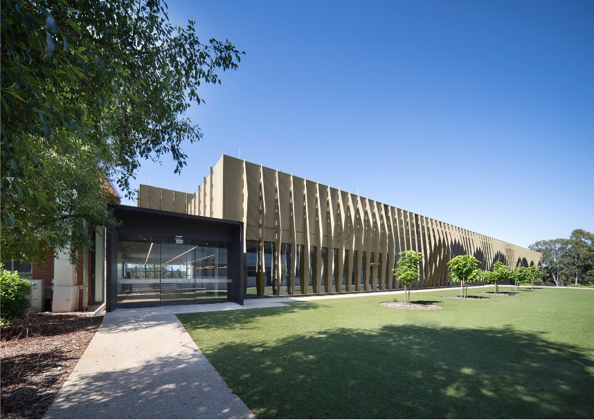
ANFF ACT
Overview
ANFF-ACT facility provides a range of capabilities and services for the micro/nanofabrication of photonic and related devices as well as the fabrication of waveguides and photonic crystals.
The node, located at the Australian National University, specialises in photonic/electronic materials growth, and the processing and fabrication of devices including micro electro-mechanical systems (MEMS). These capabilities provide a range of services for the fabrication of photonic and related devices as well as the production of waveguides and photonic crystals.
ANFF-ACT works closely with two renowned research groups based at ANU’s Laser Physics Centre and the Department of Electronic Materials Engineering. These groups bring expertise in the capabilities of high-energy ion implantation, Si-etching, optical characterisation and two metal organic chemical vapour deposition (MOCVD) reactors for the growth of III-V compound semiconductor multilayers based on: GaAs, AIGaAs, InGaAs, InP, InGaAsP, InAlGaAs, GaSb, InSb, InGaAsN. These reactors enable the fabrication of nanowires, quantum dots, quantum wells, strained layers and devices.
ANFF-ACT facilities provide a dynamic, exciting and collaborative atmosphere where researchers can get the most from their ideas with the best possible support and world class equipment.
Services include the scale-up prototyping of devices such as organic solar cells, organic light emitting diodes, organic circuit elements, microfluidic devices, bioassay platforms, biomaterial scaffolds, microbioreactors and production of materials for microelectronics to semiconductor-industry standards.
Node Competencies
Specialist fields: micro/nano fabrication of photonic and related devices; fabrication of waveguides and photonic crystals; Micro electro-mechanical systems (MEMS).
Flagship facilities: Electron beam lithography (EBL); sputtering system for metal and dielectric multi-layer deposition; Cluster tool for dry etching and deposition; Dual beam focused ion beam; Nano imprint lithography.
Contact
Node Director: Prof Hoe Tan
Email: Hoe.Tan@anu.edu.au
Phone: +61 2 6125 0363
Facility Manager: Dr Horst Punzmann
Email: horst.punzmann@anu.edu.au
Phone: +61 2 6125 0001

Location
Australian National University (ANU)
Address
Research School of Physics
building #160, Level 3, End of Mills Road
The Australian National University
Canberra ACT 2601
+61 2 6125 0001
Equipment
Deposition
Kurt Lesker Nano36
Thermal evaporator for depositing Au, Cu, Zn, etc.
ACT Node
Australian National University (ANU)
Technique
Thermal evaporation
Description
Thermal deposition of various materials.
Related Information
A large choice of metals is allowed. However, no toxic material's are permitted.
Tool Contact
horst.punzmann@anu.edu.au
AJA International ATC-2400 V
Sputtering system
ACT Node
Australian National University (ANU)
Technique
Sputtering
Description
Magnetron sputter system with three DC sources and three RF sources
Related Information
A large choice of materials available. Provides reactive sputtering and co-sputtering.
Tool Contact
horst.punzmann@anu.edu.au
Oxford Instruments Plasmalab 100
Plasma enhanced chemical vapour deposition system (PECVD) for depositing SiOx, SiNx, a-Si
ACT Node
Australian National University (ANU)
Technique
Plasma Enhanced Chemical Vapour Deposition (PECVD)
Description
Deposit dielectrics SiOx, SiNx and amorphous Si
Related Information
Maximum electrode/sample temperature 650°C
Tool Contact
horst.punzmann@anu.edu.au
Aixtron 200/4
MOCVD (horizontal flow) system for epitaxial growth of III-V semiconductor structures.
ACT Node
Australian National University (ANU)
Technique
Metal-Organic Chemical Vapour Deposition (MOCVD)
Description
Epitaxial growth of III-V (arsenide, phosphide and antimonide based materials) 2D and 3D semiconductor structures.
Related Information
A range of available sources (Ga, Al, In, Sn, Si, Zn, Sb and As, P) allows for the growth of wide range of semiconductor structures for various applications including metal catalysed nanostructures. Growth can be done on various substrates (GaAs, InP, InAs, GaP, Si etc.) and various crystal orientation up to 4" diameter and surface temperature up to 700C.
Tool Contact
horst.punzmann@anu.edu.au
Aixtron 3x2FT – Epitaxial growth of III-N
MOCVD CCS (Close-Coupled Showerhead) system for growth of III-nitride semiconductor structures
ACT Node
Australian National University (ANU)
Technique
Metal-Organic Chemical Vapour Deposition (MOCVD)
Description
Epitaxial growth of III-N (nitride based materials) 2D and 3D semiconductor structures.
Related Information
A range of available sources (Ga, Al, In, B, Si, Mg, N) allows for the growth of wide range of semiconductor structures for various applications. Growth can be done on various substrates (Sapphire, Si, etc.) and various crystal orientation up to 4" diameter and surface temperature up to 1300C.
Tool Contact
horst.punzmann@anu.edu.au
Aixtron 3x2FT – Epitaxial growth of III-V
MOCVD CCS (Close-Coupled Showerhead) system for growth of III-V (III-As, III-P, III-Sb) semiconductor structures
ACT Node
Australian National University (ANU)
Technique
Metal-Organic Chemical Vapour Deposition (MOCVD)
Description
Epitaxial growth of III-V (arsenide, phosphide and antimonide based materials) 2D and 3D semiconductor structures.
Related Information
A range of available sources (Ga, Al, In, C, Si, Mg, Zn, Sb and As, P in hydride and alkyl forms) allows for the growth of wide range of semiconductor structures for various applications. Growth can be done on various substrates (GaAs, InP, InAs, GaP, Si etc.) and various crystal orientation up to 4" diameter and surface temperature up to 800C.
Tool Contact
horst.punzmann@anu.edu.au
Temescal BJD2000
Electron beam evaporator for depositing metals including Au, Pt, Ti, Al, Cr, Ge, Ni, Mo, Nb
ACT Node
Australian National University (ANU)
Technique
Electron Beam Evaporation (E-Beam Evaporation)
Description
Equipment provides E-beam evaporation of metals and also features a thermal evaporation source for gold.
Related Information
Features an electron gun and up to six crucibles. Materials: Au, Pt, Ag, Ti, Cr, Al, Ge, Ni, Mo
Tool Contact
horst.punzmann@anu.edu.au
Picosun Sunale
Atomic layer deposition (ALD) system for depositing Al, Zn, Ti, Hf, Ta, Si oxides and TiN
ACT Node
Australian National University (ANU)
Technique
Atomic Layer Deposition (ALD)
Description
Load-locked ALD system with thermal and plasma ALD processes
Related Information
Sources for: Ti, Zn, Al, Si, Hf, Ta, Zr
Tool Contact
horst.punzmann@anu.edu.au
TOOL MAKE AND MODEL
KEY DIFFERENTIATOR
LOCATION
TOOL MAKE AND MODEL
KEY DIFFERENTIATOR
LOCATION
Kurt Lesker Nano36
Thermal evaporator for depositing Au, Cu, Zn, etc.
ACT Node
Australian National University (ANU)
Description
Thermal deposition of various materials.
Related Information
A large choice of metals is allowed. However, no toxic material's are permitted.
Tool Contact
horst.punzmann@anu.edu.au
TOOL MAKE AND MODEL
KEY DIFFERENTIATOR
LOCATION
AJA International ATC-2400 V
Sputtering system
ACT Node
Australian National University (ANU)
Description
Magnetron sputter system with three DC sources and three RF sources
Related Information
A large choice of materials available. Provides reactive sputtering and co-sputtering.
Tool Contact
horst.punzmann@anu.edu.au
TOOL MAKE AND MODEL
KEY DIFFERENTIATOR
LOCATION
Oxford Instruments Plasmalab 100
Plasma enhanced chemical vapour deposition system (PECVD) for depositing SiOx, SiNx, a-Si
ACT Node
Australian National University (ANU)
Description
Deposit dielectrics SiOx, SiNx and amorphous Si
Related Information
Maximum electrode/sample temperature 650°C
Tool Contact
horst.punzmann@anu.edu.au
TOOL MAKE AND MODEL
KEY DIFFERENTIATOR
LOCATION
Aixtron 200/4
MOCVD (horizontal flow) system for epitaxial growth of III-V semiconductor structures.
ACT Node
Australian National University (ANU)
Description
Epitaxial growth of III-V (arsenide, phosphide and antimonide based materials) 2D and 3D semiconductor structures.
Related Information
A range of available sources (Ga, Al, In, Sn, Si, Zn, Sb and As, P) allows for the growth of wide range of semiconductor structures for various applications including metal catalysed nanostructures. Growth can be done on various substrates (GaAs, InP, InAs, GaP, Si etc.) and various crystal orientation up to 4" diameter and surface temperature up to 700C.
Tool Contact
horst.punzmann@anu.edu.au
TOOL MAKE AND MODEL
KEY DIFFERENTIATOR
LOCATION
Aixtron 3x2FT – Epitaxial growth of III-N
MOCVD CCS (Close-Coupled Showerhead) system for growth of III-nitride semiconductor structures
ACT Node
Australian National University (ANU)
Description
Epitaxial growth of III-N (nitride based materials) 2D and 3D semiconductor structures.
Related Information
A range of available sources (Ga, Al, In, B, Si, Mg, N) allows for the growth of wide range of semiconductor structures for various applications. Growth can be done on various substrates (Sapphire, Si, etc.) and various crystal orientation up to 4" diameter and surface temperature up to 1300C.
Tool Contact
horst.punzmann@anu.edu.au
TOOL MAKE AND MODEL
KEY DIFFERENTIATOR
LOCATION
Aixtron 3x2FT – Epitaxial growth of III-V
MOCVD CCS (Close-Coupled Showerhead) system for growth of III-V (III-As, III-P, III-Sb) semiconductor structures
ACT Node
Australian National University (ANU)
Description
Epitaxial growth of III-V (arsenide, phosphide and antimonide based materials) 2D and 3D semiconductor structures.
Related Information
A range of available sources (Ga, Al, In, C, Si, Mg, Zn, Sb and As, P in hydride and alkyl forms) allows for the growth of wide range of semiconductor structures for various applications. Growth can be done on various substrates (GaAs, InP, InAs, GaP, Si etc.) and various crystal orientation up to 4" diameter and surface temperature up to 800C.
Tool Contact
horst.punzmann@anu.edu.au
TOOL MAKE AND MODEL
KEY DIFFERENTIATOR
LOCATION
Temescal BJD2000
Electron beam evaporator for depositing metals including Au, Pt, Ti, Al, Cr, Ge, Ni, Mo, Nb
ACT Node
Australian National University (ANU)
Description
Equipment provides E-beam evaporation of metals and also features a thermal evaporation source for gold.
Related Information
Features an electron gun and up to six crucibles. Materials: Au, Pt, Ag, Ti, Cr, Al, Ge, Ni, Mo
Tool Contact
horst.punzmann@anu.edu.au
TOOL MAKE AND MODEL
KEY DIFFERENTIATOR
LOCATION
Picosun Sunale
Atomic layer deposition (ALD) system for depositing Al, Zn, Ti, Hf, Ta, Si oxides and TiN
ACT Node
Australian National University (ANU)
Description
Load-locked ALD system with thermal and plasma ALD processes
Related Information
Sources for: Ti, Zn, Al, Si, Hf, Ta, Zr
Tool Contact
horst.punzmann@anu.edu.au
Etching
SAMCO ICP-RIE 400iP – plasma etch no metals
Cl- ICP-RIE for etching III-V semiconductors
ACT Node
Australian National University (ANU)
Technique
Reactive Ion Etching (RIE)
Description
Inductively Coupled plasma etch tool for etching III-V semiconductors, no metals etching
Related Information
Available gases: Cl2, BCl3, SiCl4, H2, O2, Ar - Electrode/sample heating up to 200°C
Tool Contact
horst.punzmann@anu.edu.au
SAMCO ICP-RIE 400iP
F-based ICP-RIE for etching SiOx, SiNx, Si
ACT Node
Australian National University (ANU)
Technique
Reactive Ion Etching (RIE)
Description
Inductively Coupled plasma etch tool for etching SiOx, SiNx, Si, Ge, etc
Related Information
Available gases: CHF3, SF6, H2, CH4, O2, Ar - Electrode/sample at 20°C
Tool Contact
horst.punzmann@anu.edu.au
TOOL MAKE AND MODEL
KEY DIFFERENTIATOR
LOCATION
TOOL MAKE AND MODEL
KEY DIFFERENTIATOR
LOCATION
SAMCO ICP-RIE 400iP – plasma etch no metals
Cl- ICP-RIE for etching III-V semiconductors
ACT Node
Australian National University (ANU)
Description
Inductively Coupled plasma etch tool for etching III-V semiconductors, no metals etching
Related Information
Available gases: Cl2, BCl3, SiCl4, H2, O2, Ar - Electrode/sample heating up to 200°C
Tool Contact
horst.punzmann@anu.edu.au
TOOL MAKE AND MODEL
KEY DIFFERENTIATOR
LOCATION
SAMCO ICP-RIE 400iP
F-based ICP-RIE for etching SiOx, SiNx, Si
ACT Node
Australian National University (ANU)
Description
Inductively Coupled plasma etch tool for etching SiOx, SiNx, Si, Ge, etc
Related Information
Available gases: CHF3, SF6, H2, CH4, O2, Ar - Electrode/sample at 20°C
Tool Contact
horst.punzmann@anu.edu.au
Laboratory Infrastructure
Scitek Australia Pty Ltd N2 Glove Box
N2 Glove Box
ACT Node
Australian National University (ANU)
Technique
Gloveboxes
Description
Storing Chemicals in N2 environment
Related Information
Used to fill ALD sources
Tool Contact
horst.punzmann@anu.edu.au
TOOL MAKE AND MODEL
KEY DIFFERENTIATOR
LOCATION
TOOL MAKE AND MODEL
KEY DIFFERENTIATOR
LOCATION
Scitek Australia Pty Ltd N2 Glove Box
N2 Glove Box
ACT Node
Australian National University (ANU)
Description
Storing Chemicals in N2 environment
Related Information
Used to fill ALD sources
Tool Contact
horst.punzmann@anu.edu.au
Lithography
EVG 620
UV lithography and NIL exposure
ACT Node
Australian National University (ANU)
Technique
Nano Imprint Lithography
Description
Standard optical lithography and Nano-Imprint UV Lithography
Related Information
Process pieces up to 6 inch wafer with 1 micron resolution. Offers top-side alignment.
Tool Contact
horst.punzmann@anu.edu.au
EVG 520
Hot embossing and wafer bonding
ACT Node
Australian National University (ANU)
Technique
Hot embossing
Description
Hot Embossing, Nanoimpint lithography, and wafer bonding
Related Information
Process up to a 6 inch wafer, 500 degrees C max temperature.
Tool Contact
horst.punzmann@anu.edu.au
FEI Helios NanoLab 600 Dual Beam SEM/FIB
Scanning electron microscope with focused ion beam for milling (FIB-SEM)
ACT Node
Australian National University (ANU)
Technique
Focused Ion Beam (FIB) milling
Description
A multifunction system for nanofabrication, characterisation, and high-resolution imaging
Related Information
Offers high-resolution imaging, milling, patterning, EDS, EBSD and EBIC
Tool Contact
horst.punzmann@anu.edu.au
Raith 150
Electron beam lithography (EBL) system
ACT Node
Australian National University (ANU)
Technique
Electron Beam Lithography (EBL)
Description
Electron-beam lithography tool for sub-µm features, accurate positioning
Related Information
30kV acceleration voltage, fixed beam moving stage, writing field up to 800x800 µm2
Tool Contact
horst.punzmann@anu.edu.au
Tepla Gigabatch 300
Plasma asher
ACT Node
Australian National University (ANU)
Technique
Cleaning
Description
Used to strip resist and clean samples.Useful during the fabrication of photovoltaic, optoelectronic or nano-photonic technologies as a vital part of the complete lithography process.
Related Information
Available gases include O2 and CF4. The system is suitable to remove organic/polymers but also dielectrics including SiOx
Tool Contact
horst.punzmann@anu.edu.au
TOOL MAKE AND MODEL
KEY DIFFERENTIATOR
LOCATION
TOOL MAKE AND MODEL
KEY DIFFERENTIATOR
LOCATION
EVG 620
UV lithography and NIL exposure
ACT Node
Australian National University (ANU)
Description
Standard optical lithography and Nano-Imprint UV Lithography
Related Information
Process pieces up to 6 inch wafer with 1 micron resolution. Offers top-side alignment.
Tool Contact
horst.punzmann@anu.edu.au
TOOL MAKE AND MODEL
KEY DIFFERENTIATOR
LOCATION
EVG 520
Hot embossing and wafer bonding
ACT Node
Australian National University (ANU)
Description
Hot Embossing, Nanoimpint lithography, and wafer bonding
Related Information
Process up to a 6 inch wafer, 500 degrees C max temperature.
Tool Contact
horst.punzmann@anu.edu.au
TOOL MAKE AND MODEL
KEY DIFFERENTIATOR
LOCATION
FEI Helios NanoLab 600 Dual Beam SEM/FIB
Scanning electron microscope with focused ion beam for milling (FIB-SEM)
ACT Node
Australian National University (ANU)
Description
A multifunction system for nanofabrication, characterisation, and high-resolution imaging
Related Information
Offers high-resolution imaging, milling, patterning, EDS, EBSD and EBIC
Tool Contact
horst.punzmann@anu.edu.au
TOOL MAKE AND MODEL
KEY DIFFERENTIATOR
LOCATION
Raith 150
Electron beam lithography (EBL) system
ACT Node
Australian National University (ANU)
Description
Electron-beam lithography tool for sub-µm features, accurate positioning
Related Information
30kV acceleration voltage, fixed beam moving stage, writing field up to 800x800 µm2
Tool Contact
horst.punzmann@anu.edu.au
TOOL MAKE AND MODEL
KEY DIFFERENTIATOR
LOCATION
Tepla Gigabatch 300
Plasma asher
ACT Node
Australian National University (ANU)
Description
Used to strip resist and clean samples.Useful during the fabrication of photovoltaic, optoelectronic or nano-photonic technologies as a vital part of the complete lithography process.
Related Information
Available gases include O2 and CF4. The system is suitable to remove organic/polymers but also dielectrics including SiOx
Tool Contact
horst.punzmann@anu.edu.au
Materials Synthesis and Modification
Ion Implantation Lab
We offer a full range of ion-implantation services Species: Most elements, except inert gases. Energies: Ion energies in the range 15 keV to 10 MeV, depending on species. Temperature: Samples can be heated or cooled during implantation. Area: Wafers up to 150 mm (6”) diameter can be accommodated. Typical implant areas are of order 3cm x 3cm.
ACT Node
Technique
Ion implantation, doping and diffusion
Description
.7 MV NEC Tandem (5SDH) high-energy ion-implanter 150 kV ion-implanter with negative ion source 1.7 MV NEC Tandem RBS/ERDA beamline for ion-beam analysis
Tool Contact
iilab@anu.edu.au
Jipelec JetFirst
Rapid thermal annealer
ACT Node
Australian National University (ANU)
Technique
Annealing
Description
To anneal and bake semiconductors or polymer samples.Maximum temperature: 1,400 degrees C (5 minutes max, lower temperatures up to 15 minutes max).
Related Information
Available gases include O2 and CF4. The system is suitable to remove organic/polymers but also dielectics including SiOx
Tool Contact
horst.punzmann@anu.edu.au
TOOL MAKE AND MODEL
KEY DIFFERENTIATOR
LOCATION
TOOL MAKE AND MODEL
KEY DIFFERENTIATOR
LOCATION
Ion Implantation Lab
We offer a full range of ion-implantation services Species: Most elements, except inert gases. Energies: Ion energies in the range 15 keV to 10 MeV, depending on species. Temperature: Samples can be heated or cooled during implantation. Area: Wafers up to 150 mm (6”) diameter can be accommodated. Typical implant areas are of order 3cm x 3cm.
ACT Node
Australian National University (ANU)
Description
.7 MV NEC Tandem (5SDH) high-energy ion-implanter 150 kV ion-implanter with negative ion source 1.7 MV NEC Tandem RBS/ERDA beamline for ion-beam analysis
Related Information
Tool Contact
iilab@anu.edu.au
TOOL MAKE AND MODEL
KEY DIFFERENTIATOR
LOCATION
Jipelec JetFirst
Rapid thermal annealer
ACT Node
Australian National University (ANU)
Description
To anneal and bake semiconductors or polymer samples.Maximum temperature: 1,400 degrees C (5 minutes max, lower temperatures up to 15 minutes max).
Related Information
Available gases include O2 and CF4. The system is suitable to remove organic/polymers but also dielectics including SiOx
Tool Contact
horst.punzmann@anu.edu.au
Packaging
Westbond 747677E
Ultrasonic/Thermosonic Gold wire bonding
ACT Node
Australian National University (ANU)
Technique
Wire bonding
Description
Wire Bonding
Related Information
Ball and Wedge bonding to gold pads
Tool Contact
horst.punzmann@anu.edu.au
EVG 520
Hot embossing and wafer bonding
ACT Node
Australian National University (ANU)
Technique
Hot embossing
Description
Hot Embossing, Nanoimpint lithography, and wafer bonding
Related Information
Process up to a 6 inch wafer, 500 degrees C max temperature.
Tool Contact
horst.punzmann@anu.edu.au
Finetech Fineplacer Lambda
Flip chip bonder
ACT Node
Australian National University (ANU)
Technique
Wafer bonding
Description
Used to align and place/bond chips on PCB or larger chips using metal bonding
Related Information
0.5 micron placement accuracy. Substrate temperature 400 degrees C. Thermocompression bonding.
Tool Contact
horst.punzmann@anu.edu.au
TOOL MAKE AND MODEL
KEY DIFFERENTIATOR
LOCATION
TOOL MAKE AND MODEL
KEY DIFFERENTIATOR
LOCATION
Westbond 747677E
Ultrasonic/Thermosonic Gold wire bonding
ACT Node
Australian National University (ANU)
Description
Wire Bonding
Related Information
Ball and Wedge bonding to gold pads
Tool Contact
horst.punzmann@anu.edu.au
TOOL MAKE AND MODEL
KEY DIFFERENTIATOR
LOCATION
EVG 520
Hot embossing and wafer bonding
ACT Node
Australian National University (ANU)
Description
Hot Embossing, Nanoimpint lithography, and wafer bonding
Related Information
Process up to a 6 inch wafer, 500 degrees C max temperature.
Tool Contact
horst.punzmann@anu.edu.au
TOOL MAKE AND MODEL
KEY DIFFERENTIATOR
LOCATION
Finetech Fineplacer Lambda
Flip chip bonder
ACT Node
Australian National University (ANU)
Description
Used to align and place/bond chips on PCB or larger chips using metal bonding
Related Information
0.5 micron placement accuracy. Substrate temperature 400 degrees C. Thermocompression bonding.
Tool Contact
horst.punzmann@anu.edu.au
Testing and validation
Bruker Dektak XT
Stylus profilometer
ACT Node
Australian National University (ANU)
Technique
Stylus profilometry
Description
Instrument used to measure height steps, typically after lithography or etching
Related Information
System accuracy down to 10 nm
Tool Contact
horst.punzmann@anu.edu.au
J. A. Woollam M-2000-DI
Spectral Ellipsometer
ACT Node
Australian National University (ANU)
Technique
Spectroscopic ellipsometry
Description
Fully automated spectral ellipsometer to measure refractive index and thickness of materials.
Related Information
Spectral Range of 193 to 1,700 nm.
Tool Contact
horst.punzmann@anu.edu.au
Custom Preparation suite
SEM coater, vacuum oven, spinners, wire bonder
ACT Node
Australian National University (ANU)
Technique
Scanning Electron Microscopy (SEM)
Description
Coating samples for SEM, vacuum oven to avoid curing polymers in air
Related Information
Various preparation equipment for samples up to 8 inches
Tool Contact
horst.punzmann@anu.edu.au
FEI Verios SEM-CL
Cathodoluminescence Analysis and Scanning Electron Microscopy (SEM-CL)
ACT Node
Australian National University (ANU)
Technique
Scanning Electron Microscopy (SEM)
Description
The FEI Verios 460L has a field emission gun and a monochromator suitable for ultra high resolution imaging. Attached to the instrument are a Gatan MonoCL4 Elite system which enables cathodoluminescence mapping and spectroscopic studies, and an Oxford electron dispersive X-ray (EDX) spectrometer for elemental analysis.
Related Information
The FEI Verios has a resolution of < 1 nm. The CL system can detect light from the UV to NIR range (200 nm - 2,000 nm) and CL can be performed at both room and low temperatures.
Tool Contact
horst.punzmann@anu.edu.au
TOOL MAKE AND MODEL
KEY DIFFERENTIATOR
LOCATION
TOOL MAKE AND MODEL
KEY DIFFERENTIATOR
LOCATION
Bruker Dektak XT
Stylus profilometer
ACT Node
Australian National University (ANU)
Description
Instrument used to measure height steps, typically after lithography or etching
Related Information
System accuracy down to 10 nm
Tool Contact
horst.punzmann@anu.edu.au
TOOL MAKE AND MODEL
KEY DIFFERENTIATOR
LOCATION
J. A. Woollam M-2000-DI
Spectral Ellipsometer
ACT Node
Australian National University (ANU)
Description
Fully automated spectral ellipsometer to measure refractive index and thickness of materials.
Related Information
Spectral Range of 193 to 1,700 nm.
Tool Contact
horst.punzmann@anu.edu.au
TOOL MAKE AND MODEL
KEY DIFFERENTIATOR
LOCATION
Custom Preparation suite
SEM coater, vacuum oven, spinners, wire bonder
ACT Node
Australian National University (ANU)
Description
Coating samples for SEM, vacuum oven to avoid curing polymers in air
Related Information
Various preparation equipment for samples up to 8 inches
Tool Contact
horst.punzmann@anu.edu.au
TOOL MAKE AND MODEL
KEY DIFFERENTIATOR
LOCATION
FEI Verios SEM-CL
Cathodoluminescence Analysis and Scanning Electron Microscopy (SEM-CL)
ACT Node
Australian National University (ANU)
Description
The FEI Verios 460L has a field emission gun and a monochromator suitable for ultra high resolution imaging. Attached to the instrument are a Gatan MonoCL4 Elite system which enables cathodoluminescence mapping and spectroscopic studies, and an Oxford electron dispersive X-ray (EDX) spectrometer for elemental analysis.
Related Information
The FEI Verios has a resolution of < 1 nm. The CL system can detect light from the UV to NIR range (200 nm - 2,000 nm) and CL can be performed at both room and low temperatures.
Tool Contact
horst.punzmann@anu.edu.au
Experts
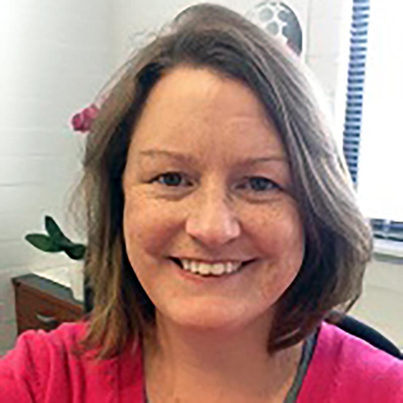
Ms Sue Berkeley
Node Administrator
Sue is in charge of liaising with users, billing, editing the website and producing the ANFF ACT Newsletter.
Read More
Australian National University (ANU)
Contact Ms Sue Berkeley
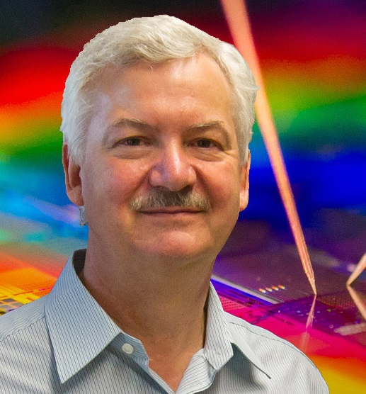
Prof Rob Elliman
Director
Rob Elliman is an Emeritus Professor of Physics in the Research School of Physics at the Australian National University (ANU) and Director of the ANU ion-implantation Laboratory (iiLab), a node of the NCRIS Heavy Ion Accelerator Capability. His fields of research include: nanotechnology; semiconductor materials science, oxide-based electronics, memristive-switching in transition-metal oxides, ion-implantation and ion-beam modification of materials.
For information on the new Ion Implantation Lab, please click on the following link.
ANU ion implantation Lab (iilab.edu.au)
Read More
Australian National University (ANU)
Contact Prof Rob Elliman
Dr Olivier Lee Cheong Lem
SEM-CL Officer
Olivier trains and assists users with SEM-CL, while supporting FIB, EBL, ALD activities
Read More
Australian National University (ANU)
Contact Dr Olivier Lee Cheong Lem